We provide precision metal components using materials such as SUS, Al, Ti, and Invar. These products are manufactured through a combination of technologies, including laser processing, high-precision photomask and etching, and precision electroforming. Our products are widely used as vapor deposition masks, encoders, electronic component assembly jigs, precision washers, and more. In addition to thin, stand-alone metal parts, we also offer products that have undergone processes such as bending, bonding, black plating, and other treatments.
Metal Laser Processing
In laser processing, a YAG laser is directed onto a metal plate to melt and penetrate the material, creating patterns. Since no photomasks are required, this method is recommended for small-batch production. The line width accuracy is ±10um.
Examples of Production by Metal Laser Processing
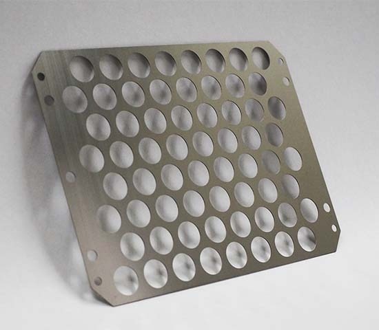
Patterns ranging from 100 to 500μm are created on 0.1mm thick SUS304 material. It is recommended to use a metal thickness that matches the minimum line width.
This is an enlarged view of the opening of the laser-processed part. The corner radius is approximately 12um.
Photo-Etching of Metals
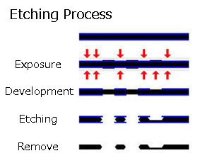
Photo-etching technology is a precision manufacturing process that enables the production of complex and fine shapes with high accuracy, short lead times, and low costs, without the use of molds. It is compatible with a variety of metals, including SUS, Al, Ti, Cu, and Invar. These metals can also be processed using half-etching. Additionally, we provide metal products with high aspect ratios using our unique techniques.
Examples of Production by Photo-Etching of Metals
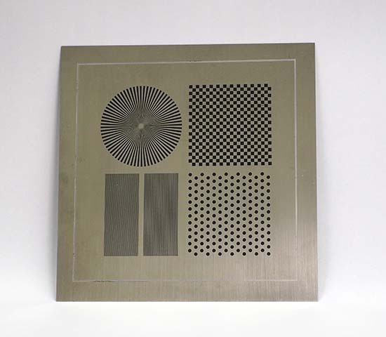
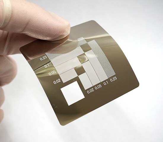
This is a SUS mask. This product is patterned using metal etching. The thickness of the SUS material is 0.3mm.
This is a gradient-type SUS mask with rectangles arranged in gradually increasing sizes. The thinnest line width is approximately 14um. The thickness of the SUS material is selected according to the line width of the pattern.
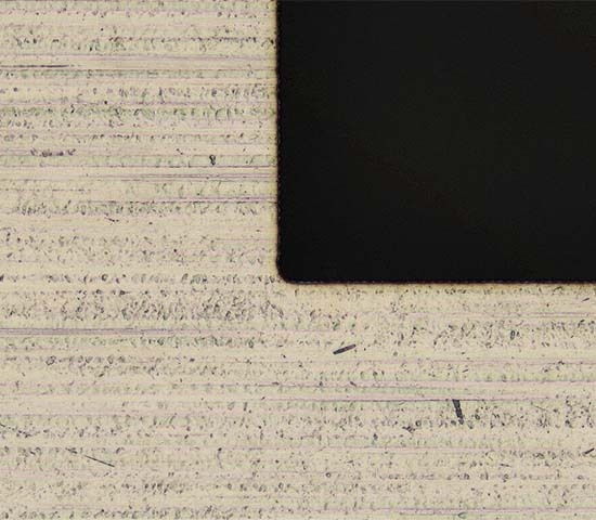
This product is made by half-etching SUS material and applying black paint to the processed areas. Half-etching is used for reflective charts, product numbering, and other applications.
Nickel Electroforming
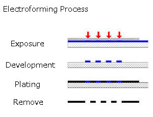
Nickel electroforming technology allows for the precise manufacturing of shapes and fine details that are impossible to produce with photo-etching. In electroforming, the shape is transferred from the resist pattern, enabling extremely high processing precision.
Examples of production using Nickel Electroforming
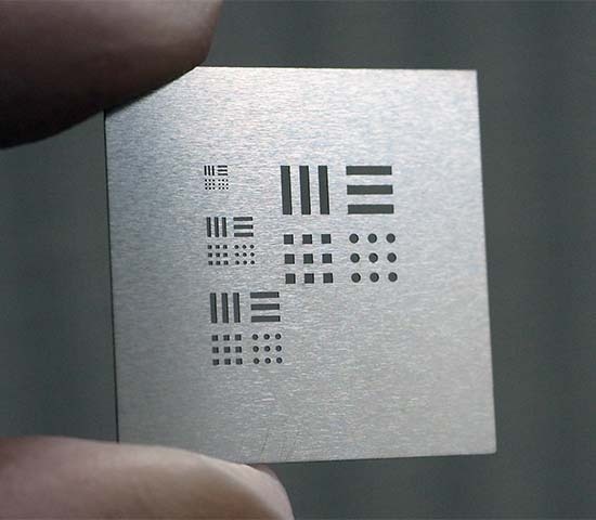
This is a product that expresses the resolution pattern through electroforming.
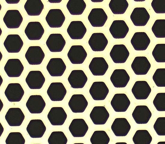
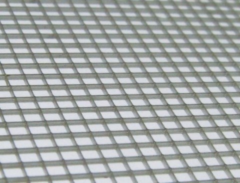
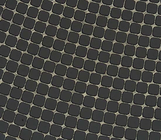
This is a product with a honeycomb pattern, where the nickel section is 20um and the pitch is 60um.