本文へ移動

Photomasks

At EQUA, we help our customers take the first step toward product creation
 
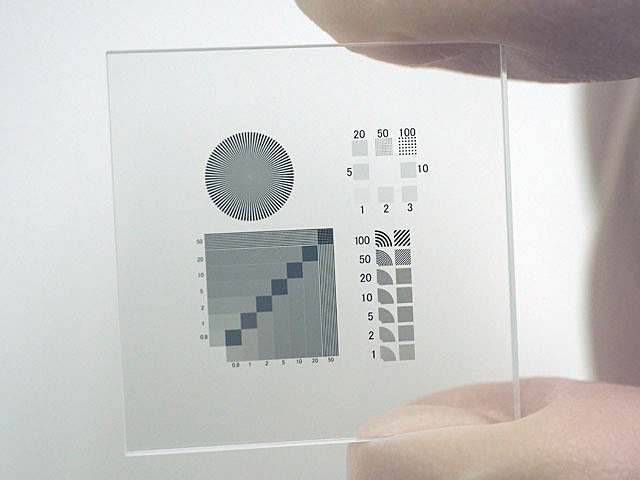
The photomasks that we provide are primarily imaged using the latest equipment, with lasers as the light source. Based on our many years of rich experience in precision photolithography, along with our proprietary pattern processing technology, we can satisfy a variety of customer needs in such fields as electronics, optical components, scales, and displays.
At EQUA, we create data from diagrams, and we help our customers make their ideas and concepts a reality.

What is a Photomask?

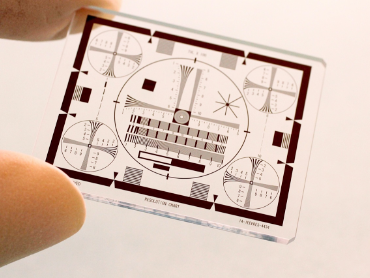
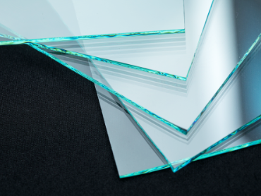
Photomasks are original sheets which are used when exposing wafers, glass substrates, printed wiring boards, metal plates, and the like to light in order to imprint patterns for electronic circuits, display devices, optical components, and precision devices. The patterns imaged on photomasks are used for a multitude of electrical products, semiconductors, televisions, smartphones, noise filters, scales, and network line-related products.
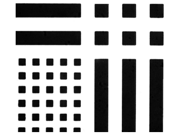
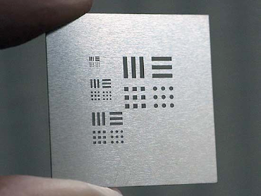
5 µm, 10 µm Patterns
φ2 µm dots
φ2 µm dots
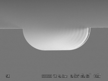
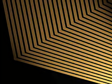
1 µm curved line
1 µm curved line

Applications / Uses

 The photomasks provided by EQUA are primarily utilized in the following areas. 
 
  • Printed wiring boards and IC packages
  • Display devices such as liquid crystal displays and touch panels
  • Optical filters
  • Optical waveguides
  • Scales and encoders
Display Devices
Display Devices 
Print Wiring Board
PWB
EQUA Co.,Ltd.
Yutaka Bldg. 5F, 8-10-6 Sagami-Ono, Minami-ku, Sagamihara, Kanagawa 252-0303, Japan

Tel: +81-42-745-2027
Fax: +81-42-745-2047

・Photomasks
・Precision Thin Film Products
・Optical Components
・Precision Metal Components

TOPへ戻る