Photomasks are original sheets which are used when exposing wafers, glass substrates, printed wiring boards, metal plates, and the like to light in order to imprint patterns for electronic circuits, display devices, optical components, and precision devices. The patterns imaged on photomasks are used for a multitude of electrical products, semiconductors, televisions, smartphones, noise filters, scales, and network line-related products.
The photomasks that we provide are primarily imaged using the latest equipment, with lasers as the light source. Based on our many years of rich experience in precision photolithography, along with our proprietary pattern processing technology, we can satisfy a variety of customer needs in such fields as electronics, optical components, scales, and displays.
There are two types of photomasks: glass masks and film masks. We also have a variety of sizes available, so we can advise you on the best fit for your application and price.
CAD

CAD is one of the important processes for establishing the optimal manufacturing process when creating precision thin film products.
The design technology cultivated at EQUA is utilized and developed to create a wide variety of products, with a focus on CAD processes.
Bring Concepts to Life

Equa creates data from drawings and supports customers in realizing their images and concepts. The drawings you provide can even be simple rough sketches. We also support a variety of applications when providing materials. Please feel free to contact us.
[Main data format]
DXF, DWG, GDSⅡ, GERBER, BMP, TIF, PDF, Ai
Design A Gradation Pattern

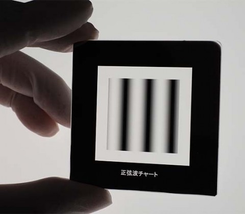
At Equa, it is possible to design a gradation pattern based on the density and transmittance desired by the customer. We can handle not only uniform changes but also sine waves, parabolas, and free density changes.
The change values you provide can be simple numbers, formulas, table data, etc. Please feel free to contact us.

Production Process

For photomasks, we implement a 24-hour production system and deliver the best possible lead time. We also continuously maintain a lineup of the latest equipment, meeting the quality requirements of customers in a wide variety of fields.
Manufacturing Process Flow
■CAD Process | Transfer
data / drawing |
↓ | |
Check specification & pattern | |
↓ | |
Pattern correction
& layout |
■ Data Format
DXF, DWG, GDSII, GERBER, BMP, TIF, and the like many other data format.
■ Pattern Formation
Straight lines, circles, arcs, sine waves, spirals, random patterns, and the like can be laid out.
■ Pattern Correction
Flexible pattern correction that fits the process is performed.
■ Uses
Precise photolithography for sensors, displays, encoders, semiconductor packages, and the like.
■Production Process | (1) Conversion of CAD data Conversion of CAD data to imaging data | ||
↓ | |||
(2) Writing Patterning by laser imaging device | |||
↓ | |||
(3) Development /Etch Developing/etching/resist stripping/cleaning process | |||
↓ | |||
(4) Measurement Measurement of line width and long dimensions using a laser interferometer or the like | |||
↓ | |||
(5) Inspenction Visual inspection of pattern using AOI or other automatic defect detection equipment | |||
↓ | |||
(6) Cleaning Mask surface cleaning and drying process | |||
↓ | |||
*1 Mounting
Pellicle | ↓ | *3 Hard
Coating | |
↓ | ↓ | ↓ | |
*2 Particle
Check | ↓ | *4 Visual
Inspection | |
↓ | ↓ | ↓ | |
(7) Final Inspection Final inspection prior to shipping | |||
↓ | |||
(8) Packing Packing into custom case, and shipping | |||
■ Options
*1. Mounting of customized pellicle suited to the exposure device
*2. Particle check after mounting pellicle
*3. Application of hard coating liquid to protect mask surface
*4. Visual inspection after application of hard coating liquid


