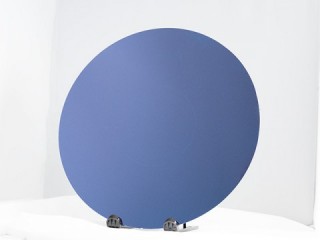
At EQUA, we offer products with multilayer patterns formed by various metal films on glass substrates and silicon wafers. We propose the optimal process by leveraging advanced processing technologies, including our unique pattern data generation techniques, high-precision mask imaging equipment, semiconductor steppers, photo-etching, lift-off, plating, and sandblasting. We also enable ultra-high-precision processing by using photomask manufacturing equipment to directly pattern onto the substrate. We can form electronic circuits using various metal thin films, such as chrome, aluminum, titanium, and ITO, on substrates like glass, ceramics, and silicon.
Substrates
- Glass
Soda lime
Quartz
Alkali-free glass
- Wafer
Silicon wafer
Compound semiconductor
- Silicon Carbide (SiC) Wafer
- Gallium Nitride (GaN) Wafer
- Printed Circuit Board
List of Glass Wafer
Specifications | |||||
Size | 4in. / 100mm | 5in. / 125mm | 6in. / 150mm | 8in. / 200mm | 12in. / 300mm |
Thickness | Available for selection | ||||
Flat / Notch | 32.5mm | 42.5mm | 57.5mm | Notch | Notch |
Surface Finish | Polished | ||||
Film Deposition | Various target deposition | ||||
Patterning | Film deposition patterning / Glass etching | ||||
Others | Any size (2in+), any shape (e.g., rectangular) | ||||
List of Bare Silicon Wafer
Specifications | |||||
Size | 4in. / 100mm | 5in. / 125mm | 6in. / 150mm | 8in. / 200mm | 12in. / 300mm |
Thickness | 525 um | 625 um | 625 um | 725 um | 775 um |
Flat/Notch | 32.5mm | 42.5mm | 57.5mm | Notch | Notch |
Type/Dopant | P/N | ||||
Orientation | (100) / (110) / (111) | ||||
Surface Finish | Polished / Etched | Polished / Polished | |||
List of Film Deposition Wafer
Specifications | |||||
Size | 4in. / 100mm | 5in. / 125mm | 6in. / 150mm | 8in. / 200mm | 12in. / 300mm |
Thickness | 525 um | 625 um | 625 um | 725 um | 775 um |
Flat / Notch | 32.5mm | 42.5mm | 57.5mm | Notch | Notch |
Type / Dopant | P/N | ||||
Orientation | (100) / (110) / (111) | ||||
Surface Finish | Polished / Etched | Polished / Etched | |||
Deposition Method | Thermal Oxide Film / Sputtering / LP-CVD / PE-CVD / ALD | ||||
Thickness | 100 ~ 10000Å | ||||
Deposition | SiO2 / SiN / P-TEOS / SiON / SiOC / HfO2 / Al / Al-Cu / Au / Pt / Cu / Cr / Ti / Ta / W / Pd / TiN / TaN / AlN / TiC / WC / ITO / SnO2 / ZnO / Ru / Ag-Pd / Co | ||||
Patterning
Patterning Details
- Pattern Process: Photolithography
- Silicon wafer processing up to 12-inch size
- From 1x photolithography to steppers


